Laser structuring of thin film sensors on technical surfaces
Thin-film strain sensors integrated in technical surfaces enable static and dynamic forces, as well as moments acting on the component, to be recorded. The operating principle is based on the piezoresistive effect: deformation of the component leads to a proportional change in the electrical resistance of a measuring grid, which is applied to the component surface.
While this principle has already been known for a long time and, for example, is used in the form of applied foil strain gages, technical implementation for the production of integrated sensors within series production parts still represents a challenge, especially where long service life, low long-term drift and high resistance to external influences are required. The manufacturing process examined in this project is based on thin-film technologies, where the sensor structure is deposited directly on the component and is therefore an integral part of the surface (see Figure 1). This creates a very compact design with a total thickness of just a few microns allowing problems that occur due to the use of polymers in traditionally bonded foil sensors (drift due to temperature or humidity effects), to be circumvented.
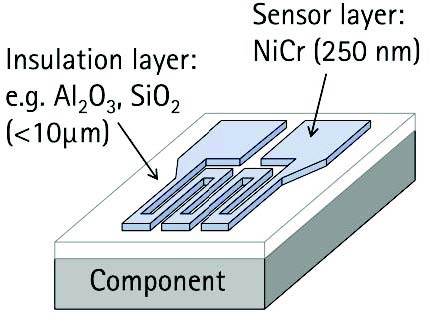


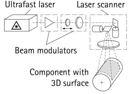
Together with the industry partner Schaeffler Technologies AG & Co. KG, the combination of processes, consisting of a full-surface coating of the component surface and subsequent selective laser structuring for generation of the measuring grid, are being investigated. This approach allows the manufacture of thin-film sensors on curved surfaces and enables diverse application scenarios, such as kerfs, indentations or shafts and other, complex component surfaces. Structuring of the sensors is performed using direct laser ablation with ultrashort laser pulses in combination with highly dynamic laser scanners. This allows high processing resolutions in the micrometer range, low processing times of typically a few seconds and high process flexibility, e.g. for trimming of measuring bridges, to be achieved. Figure 2 shows the basic structure a laser structuring system that allows for surface treatment of curved parts.


The sensors manufactured in this transfer project are used in intelligent tool machines (Figure 3) to record process forces and enable conclusions to be made concerning the machining process. The main project objectives egarding processing time, sensor quality and rejection rates are undergoing continued testing using a component from a wheel bearing, in order to make final statements about the economic viability of industrial application. Measuring grids on this demonstration component are shown in Figure 4.


Subproject leader



Industry partner


Oberflächentechnik
Industriestraße 1-3
91074 Herzogenraurach


Oberflächentechnik
Industriestraße 1-3
91074 Herzogenraurach


